Chapter 3: UART Thy Mother's Glass
I am getting a little tired of having to find an appropriate image for every blog post. Here is a picture of my UART: Universally Admired Refined Tomcat. In this picture he is transmitting some data.

Disclaimer: I do not work for Sony. Despite the disturbing percentage of my shirts, jackets, and bookbags that are PlayStation dev-related, I have never worked for Sony. I do, however, have many friends that work at Sony, some of which I hope will call off the corporate lawyers. JayStation is in no way associated with Sony or PlayStation, and any stupid things I say represent only my own ineptitude and silliness.
LEDs are nice as an initial attempt at some debugging, but what we really want is something more... illuminating... than flashing a light. I’m going to introduce the UART, show you what it can do for you, and in the next chapter show how I am using it to reload and hotswap my custom OS flash files without having to repeatedly insert and remove the MicroSD card.
The UART, in layman’s terms, is the thingy that sends the stuff over the guy. It stands for Universal Asynchronous Receiver Transmitter, and its what we are going to use to send bytes (one bit at a time) between the target and the host over serial. Hope you bought that serial to USB adaptor because here is where you start to need it.
I’m going to show you my UART code initialization code and try to explain it line by line. Lets start by making some defines for the needed register base addresses and offsets
Not too hard to understand. The start of the area where the UART registers are memory mapped to is 0x3F201000 and the defines after that are the offsets where the interesting registers live. The first half of the UART setup code looks like this
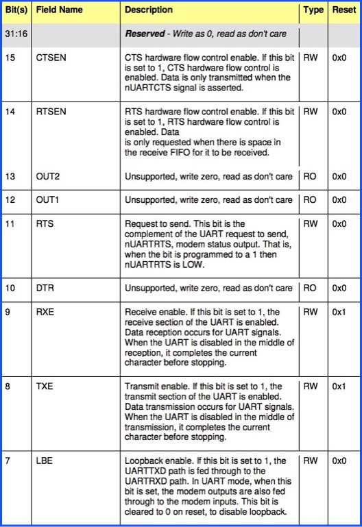
What does UART_CR (control register) look like? ARM says
Not shown is bit 0 which is the UART0 enable/disable bit. Broadcom manual page 185 says the steps to program the UART are as follows:
0) Disable the UART.
1) Wait for the end of transmission or reception of the current character
2) Flush the transmit FIFO by setting the FEN bit to 0 in the Line Control Register, UART_LCRH.
3) Reprogram the Control Register, UART_CR.
4) Enable the UART.
That explains why we start by writing a zero to UART_CR, therefore disabling it. Now we move on to those weird GPIO clock writes and delays. Again, we RTFM page 101
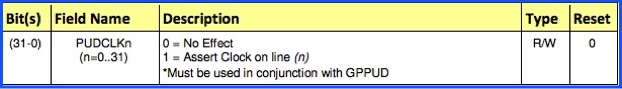
GPIO Pull-up/down Clock Registers (GPPUDCLKn)
0) Write GPPUD to set control signal (Pull-up/Pull-Down/neither to remove)
1) Wait 150 cycles – this provides the required set-up time for the control signal
2) Write to GPPUDCLK0 to clock the control signal into the GPIO pads you wish to modify
3) Wait 150 cycles – this provides the required hold time for the control signal
4) Write to GPPUD to remove the control signal
5) Write to GPPUDCLK0 to remove the clock
And that is exactly what we are doing with that business of writing zeroes to registers and delaying 150 cycles. As James Lee said, they seem to be exposing the latch semantics to the user instead of handling it behind the scenes. Since most of the writes are just for signal control, I’ll just look at the write of 0xC000 (0b1100000000000000) to GPPUDCLK0.
So as you’d expect, we are disabling pull up/down for pins 14 and 15 which by default happen to be UART TXD and RXD respectively. And if you’re wondering why we have to do all this, let us read from the book of peripheral, page 10, chapter 2, verse 1
GPIO pins should be set up first the before enabling the UART. The UART core is build to emulate 16550 behaviour. So when it is enabled any data at the inputs will immediately be received . If the UART1_RX line is low (because the GPIO pins have not been set-up yet) that will be seen as a start bit and the UART will start receiving 0x00-characters.
Onward to the second half of the setup
IBRD and FBRD are the integer baud rate divisor and fractional baud rate divisor. The manual states that the baud rate divisor is equal to the UART clock divided by 16 times the baud rate. The UART clock is 3,000,000 and the wanted baud is 115,000. Meaning 3,000,000 / (16 * 115,000) = 1.63. Since we can’t put 1.63 in the divisor register, we load the integer part 1 into r2 and store it in IBRD. Close enough isn’t good enough, so we have to take the remaining 0.63 and somehow store that in the fractional part. The fractional part can be 6 bits, ranging from 0 to 63. So to encode the fractional part, we multiply 64 by the fractional part 0.63 to get 40.32. Thats why we are writing 40 to FBRD.
LCRH is the line control register. Rather than pasting in a description of all the bits, it should be enough to say we are disabling parity and send break, enabling transmit/receive FIFOs, and setting the number of bits transmitted in a frame to 8. Don’t believe me? Broadcom manual page 184. Finally, we write a bunch of 1’s to IMSC to mask all the interrupts, and write 0x301 to the UART control register. This enables the UART and enables transmit and receive.
From this point on, all we need to do is to know how to transmit and receive actual data. All you need to do when writing is wait for the output buffer to not be full, and then write UART0_DR. To read, just wait until the receive buffer is not empty, and then read from UART0_DR. Easy peasy.
And finally, because I promised you guys some better debugging, here are a couple of self-explanatory routines I quickly hacked together for printing out strings and numbers in hex. I leave it to you to recreate printf :)
// UART
.equ UART_BASE_ADDR, 0x3F201000
.equ UART0_DR, 0x00
.equ UART0_FR, 0x18
.equ UART0_IBRD, 0x24
.equ UART0_FBRD, 0x28
.equ UART0_LCRH, 0x2C
.equ UART0_CR, 0x30
.equ UART0_IMSC, 0x38
.equ UART0_ICR, 0x44
// uart base address
ldr r0, =UART_BASE_ADDR
// GPIO base address
ldr r1, =GPIO_BASE_ADDR
// Disable UART0.
mov r2, #0
str r2, [r0, #UART0_CR]
// Setup the GPIO pin 14 && 15.
// Disable pull up/down for all GPIO pins & delay for 150 cycles.
mov r2, #0
str r2, [r1, #GPPUD]
bl delay150
// Disable pull up/down for pin 14,15 & delay for 150 cycles.
mov r2, #0xC000
str r2, [r1, #GPPUDCLK0]
bl delay150
// Write 0 to GPPUDCLK0 to make it take effect.
mov r2, #0
str r2, [r1, #GPPUDCLK0]
// Clear pending interrupts.
ldr r2, =0x7FF
str r2, [r0, #UART0_ICR]
// Set integer & fractional part of baud rate.
// Divider = UART_CLOCK/(16 * Baud)
// Fraction part register = (Fractional part * 64) + 0.5
// UART_CLOCK = 3000000; Baud = 115200 (or 38400).
// Divider = 3000000 / (16 * 115200) = 1.627 = ~1.
// Fractional part register = (.627 * 64) + 0.5 = 40.6 = ~40.
// Divider = 3000000 / (16 * 38400) = 4.883 = ~4.
// Fractional part register = (.883 * 64) + 0.5 = 57.012 = ~57.
mov r2, #4
str r2, [r0, #UART0_IBRD]
mov r2, #57
str r2, [r0, #UART0_FBRD]
// Enable FIFO & 8 bit data transmissio (1 stop bit, no parity).
mov r2, #0x70
str r2, [r0, #UART0_LCRH]
// Mask all interrupts.
//mmio_write(UART0_IMSC, (1 << 1) | (1 << 4) | (1 << 5) | (1 << 6) |
// (1 << 7) | (1 << 8) | (1 << 9) | (1 << 10));
ldr r2, =0x7F2
str r2, [r0, #UART0_IMSC]
// Enable UART0, receive & transfer part of UART.
ldr r2, =0x301
str r2, [r0, #UART0_CR]
// put char over serial
.globl js2osUartPutc
js2osUartPutc:
push {lr}
// Wait for UART to become ready to transmit.
ldr r1, =UART_BASE_ADDR
js2osUartPutcIsFull$:
ldr r2, [r1, #UART0_FR]
and r2, r2, #32
cmp r2, #0
bne js2osUartPutcIsFull$
str r0, [r1, #UART0_DR]
pop {pc}
.align 2
uart_putc_atomic_spinlock: .word 0
// get char over serial, blocking
.globl js2osUartGetc
js2osUartGetc:
// Block waiting for a byte to arrive
ldr r1, =UART_BASE_ADDR
js2osUartGetcIsEmpty$:
ldr r2, [r1, #UART0_FR]
and r2, r2, #16
cmp r2, #0
bne js2osUartGetcIsEmpty$
ldr r0, [r1, #UART0_DR]
mov pc, lr
// r0 is string pointer
.globl js2osDebugPrintString
js2osDebugPrintString:
push {r4, r5, r6, lr}
push {r0}
mov32 r0, debug_print_string_spinlock
bl js2osAtomicSpinLockAcquire
pop {r0}
// js2osUartPutc only uses r0, r1, r2, so there is no need to save r3
mov r4, r0
mov r5, #0xFF
js2osDebugPrintHexMsgAgain:
ldrb r0, [r4], #1
cmp r0, #0
beq js2osDebugPrintStringDone
bl js2osUartPutc
b js2osDebugPrintHexMsgAgain
js2osDebugPrintStringDone:
mov32 r0, debug_print_string_spinlock
bl js2osAtomicSpinLockRelease
pop {r4, r5, r6, pc}
.align 4
debug_print_string_spinlock: .word 0
.globl js2osDebugPrintNumHex
js2osDebugPrintNumHex:
push {r4, r5, lr}
mov r4, r0
push {r0}
mov32 r0, debug_print_hex_num_spinlock
bl js2osAtomicSpinLockAcquire
pop {r0}
// 0x
mov r0, #0x30
bl js2osUartPutc
mov r0, #0x78
bl js2osUartPutc
// now write out the 8 nybbles
mov r5, #28
js2osDebugPrintHexNumLoop:
lsr r0, r4, r5
and r0, r0, #0xF
cmp r0, #9
addle r0, r0, #0x30
addgt r0, r0, #0x37
bl js2osUartPutc
sub r5, r5, #4
cmp r5, #0
bge js2osDebugPrintHexNumLoop
mov32 r0, debug_print_hex_num_spinlock
bl js2osAtomicSpinLockRelease
pop {r4, r5, pc}
.align 4
debug_print_hex_num_spinlock: .word 0
.globl js2osDebugPrintStringAndNum
js2osDebugPrintStringAndNum:
push {r4, lr}
push {r0, r1}
mov32 r0, print_msg_and_value_spinlock
bl js2osAtomicSpinLockAcquire
pop {r0, r1}
mov r4, r1
bl js2osDebugPrintString
mov r0, r4
bl js2osDebugPrintNumHex
mov32 r0, print_msg_and_value_spinlock
bl js2osAtomicSpinLockRelease
pop {r4, pc}
.align 4
print_msg_and_value_spinlock: .word 0